Protoboard Designer
Free PCB Layout Editor for Makers & Hobbyists
Protoboard Designer is a free, browser-based PCB design tool — no EDA experience needed. Place components, route copper traces, and export Gerber files for fabrication or home etching. Available on Android and the web.
"Where ideas become circuits."
Free to start · No credit card required · No EDA experience needed
Everything a prototype needs. Nothing it doesn't.
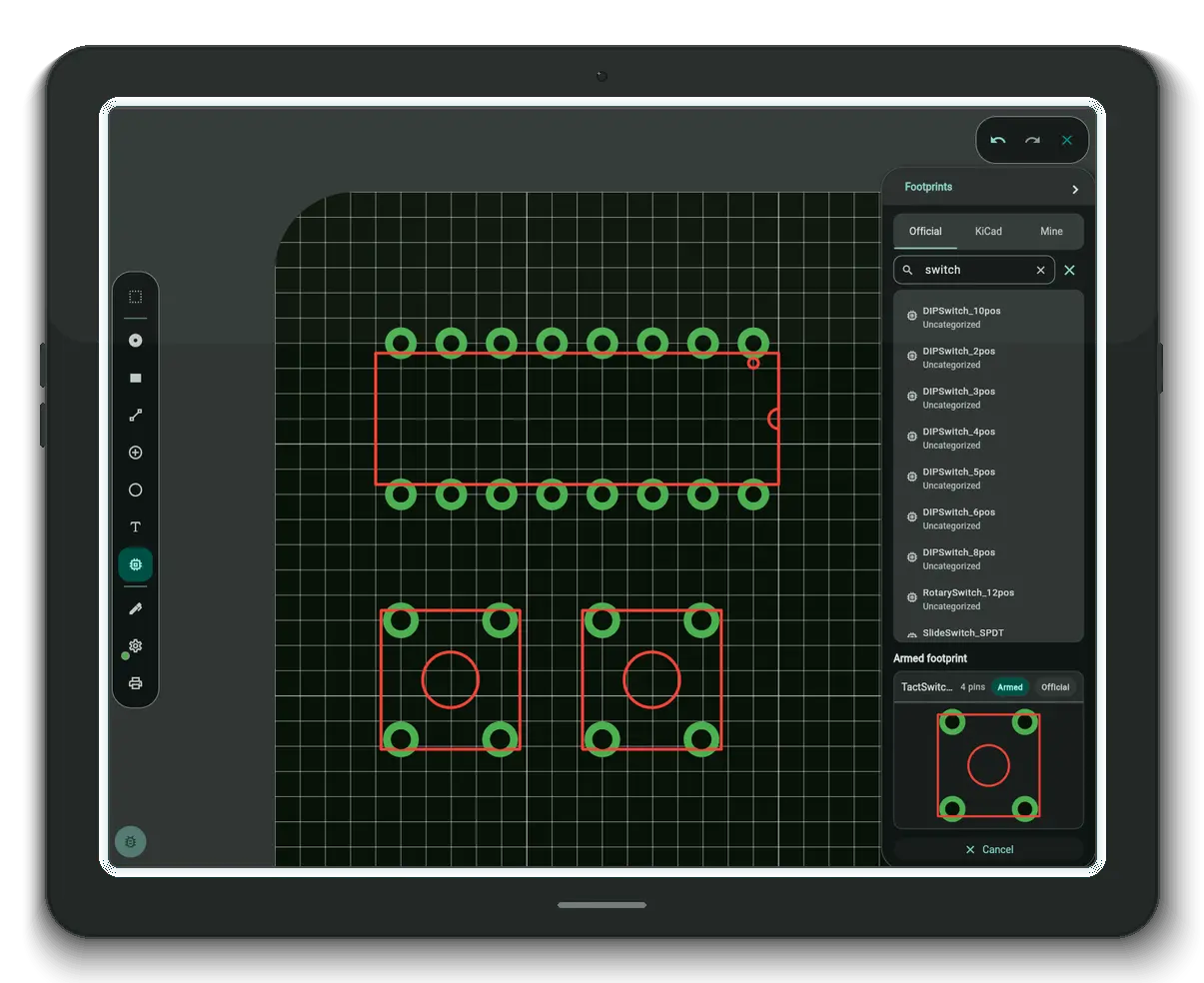
WYSIWYG Layout Editor
See exactly what you'll get. Place footprints, route copper traces, and arrange your board visually — what you see on screen is what gets fabricated. No netlist required.
Cloud Project Sync
Your projects are backed up and synced across your devices — like Dropbox for your PCBs. Pick up on your phone where you left off on the web, always with the latest version.
Gerber & PDF Export
Export Gerber files to send straight to a PCB fab, or generate a PDF to etch your own board at home. Either way, you're one tap away from something physical.
Rich Footprint Library
Start with a built-in component library, import footprints from KiCad, or add any public GitHub repository as a footprint source. Your parts, your workflow.
Not another heavy EDA suite — a KiCad alternative built for simplicity
Unlike KiCad, Eagle, or Altium — Protoboard Designer is designed to get you from idea to board in minutes, not days.
Your next circuit starts here.
Sign in with Google — no credit card required. Use the web app in your browser, or install the Android app from Google Play. Start laying out your board in seconds.